Oxide Flatlands
Institute of Solid State Physics and MAPEX Center for Materials and Processes, University of Bremen, Germany Dr. Jan Ingo Flege received his PhD in Physics at the University of Hamburg, Germany in 2004. After completing two postdoctoral positions (2004/05: University of Bremen, Germany; 2006/07: Brookhaven National Laboratory, NY, United States) he joined the group of Prof. Dr. Jens Falta at the Institute of Solid State Physics at the University of Bremen as research associate in 2008. Besides teaching, he is designing and leading the research projects targeting growth, characterization, and manipulation of transition metal and rare-earth oxides surfaces and interfaces as well as graphene.
 Reducible oxides intrinsically offer a wide range of structural, electronic, and chemical properties. In many circumstances, these materials properties may exhibit spatial variations even down to the nanometer scale, which poses a formidable challenge for the intentional growth of extended homogeneous oxide phases and nanostructures as well as their subsequent characterization, e.g., during surface chemical reactions. At the University of Bremen, we address these issues by employing low-energy electron microscopy (LEEM), a full-field imaging technique that allows monitoring of dynamic surface processes with nanometer resolution at video rates (figure 1).
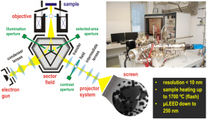
Figure 1: The low-energy electron microscope (LEEM) at Bremen University.
In this technique, the sample is irradiated by a nearly parallel beam of electrons at normal incidence with a kinetic energy of typically 15-20 keV. Close to the sample, the electrons are decelerated down to a few eV by a retarding field between the sample and the objective lens. After reflection at the sample surface, the electrons are reaccelerated, and a low-energy electron diffraction (LEED) pattern is formed in the backfocal plane of the objective. This reciprocal space image is transferred into the imaging column, where it is transformed into real space and finally projected onto the screen. In a similar fashion, the diffraction pattern can be recorded by appropriate adjustment of the projector settings. Using suitable apertures that restrict the illumination of the sample to regions down to 250 nm in diameter, even local “micro”-LEED patterns can be collected, which is especially powerful when dealing with samples exhibiting different structural features, e.g., crystallographic phases, at the nanoscale.
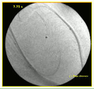
![Figure 2: (left) LEEM image and (right) LEED pattern of cerium oxide on Ru(0001).[B. Kaemena, S. D. Senanayake, A. Meyer, J. T. Sadowski, J. Falta, and J. I. Flege, J. Phys. Chem. C 117, 221 (2013)].](http://www.cost-redox.nano.cnr.it/wp-content/uploads/2012/10/ingo_fig2-300x141.png)
Figure 2: (left) LEEM image and (right) LEED pattern of cerium oxide on Ru(0001).
[B. Kaemena, S. D. Senanayake, A. Meyer, J. T. Sadowski, J. Falta, and J. I. Flege, J. Phys. Chem. C 117, 221 (2013)].
Examples for the insights that can be gained with LEEM are shown in Figure 2. In the image, a LEEM image is reproduced of cerium oxide grown on Ru(0001) by reactive molecular beam epitaxy, i.e., by depositing metallic cerium in a suitable background pressure of molecular oxygen. The cerium dioxide islands are isolated and exhibit rather well-defined sizes and shapes, which together with their areal density are all related to the growth temperature. Since these growth experiments can even be performed during microscope operation (see ceox_animated3.gif), LEEM can also provide unprecedented insights into their growth mode. Figure 2 also displays a LEED pattern that may be observed for ceria growth on ruthenium, illustrating the richness of the information that can be obtained in a LEEM instrument.
Publications resulting from joint COST funded short-term scientific missions:
M. Sauerbrey, G. Gasperi, P. Luches, J. Falta, S. Valeri, and J. I. Flege
Cerium oxide epitaxial nanostructures on Pt(111): growth, morphology and structure
Top. Catal. (2016), in press.
J. Höcker, T. Duchoň, K. Veltruská, J. Falta, V. Matolín, S. D. Senanayake, and J. I. Flege
Controlled growth of exclusively (100) oriented CeO2 nanostructures on Cu(111) surfaces
J. Phys. Chem. C 120, 4895 (2016). (journal cover from Mar 10th 2016)
J. I. Flege, J. Lachnitt, D. Mazur, P. Sutter, and J. Falta
Role of RuO2(100) in surface oxidation and CO oxidation catalysis on Ru(0001)
Phys. Chem. Chem. Phys. 18, 213 (2016).
Further publications benefiting from the COST Action CM1104:
M. Sauerbrey, J. Höcker, M. Wellbrock, M. Schowalter, J.-O. Krisponeit, K. Müller-Caspary, A. Rosenauer, G. Wei, L. Colombi Ciacchi, J. Falta, and J. I. Flege
Ultrasmooth Ru(0001) films as templates for ceria nanoarchitectures
Cryst. Growth Des. (2016), in press.
D. C. Grinter, S. D. Senanayake, and J. I. Flege
In situ growth, structure, and real-time chemical reactivity of well-defined CeOx-Ru(0001) model surfaces
Appl. Catal. B: Environmental 197, 286 (2016).
J. I. Flege, J. Höcker, B. Kaemena, T. O. Menteş, A. Sala, A. Locatelli, S. Gangopadhyay, J. T. Sadowski, S. D. Senanayake, and J. Falta
Growth and characterization of epitaxially stabilized ceria(001) nanostructures on Ru(0001)
Nanoscale 8, 10849 (2016).
J. Höcker, T. O. Menteş, A. Sala, A. Locatelli, Th. Schmidt, J. Falta, S. D. Senanayake, and J. I. Flege
Unraveling the dynamic nanoscale reducibility (Ce4+ à Ce3+) of CeOx-Ru in hydrogen activation
Adv. Mater. Interfaces 2, 1500314 (2015). (selected for journal inside cover)
J. Höcker, W. Cartas, A. Schaefer, M. Bäumer, J. Weaver, J. Falta, and J. I. Flege
Growth, structure, and stability of the high-index TbOx(112) surface on Cu(111)
J. Phys. Chem. C 119, 14175 (2015).
A. Allahgholi, J. I. Flege, S. Thieß, W. Drube, and J. Falta
Oxidation state analysis of ceria by XPS
ChemPhysChem 16, 1083 (2015).
E. E. Krasovskii, J. Höcker, J. Falta, and J. I. Flege
Surface resonances in electron reflection from overlayers
J. Phys.: Condens. Matter 27, 035501 (2015).
J. I. Flege, B. Kaemena, Th. Schmidt, and J. Falta
Epitaxial, well-ordered ceria/lanthana high-k gate dielectrics on silicon
J. Vac. Sci. Technol. B 32, 03D124 (2014).
J. I. Flege, B. Kaemena, J. Höcker, F. Bertram, J. Wollschläger, Th. Schmidt, and J. Falta
Ultrathin, epitaxial cerium dioxide on silicon
Appl. Phys. Lett. 104, 131604 (2014).
J. I. Flege, B. Kaemena, A. Meyer, J. Falta, S. D. Senanayake, J. T. Sadowski, R. D. Eithiraj, and E. E. Krasovskii
Origin of chemical contrast in low-energy electron reflectivity of correlated multivalent oxides: the case of ceria
Phys. Rev. B 88, 235428 (2013).